

Scanning Probe Microscopy (SPM)
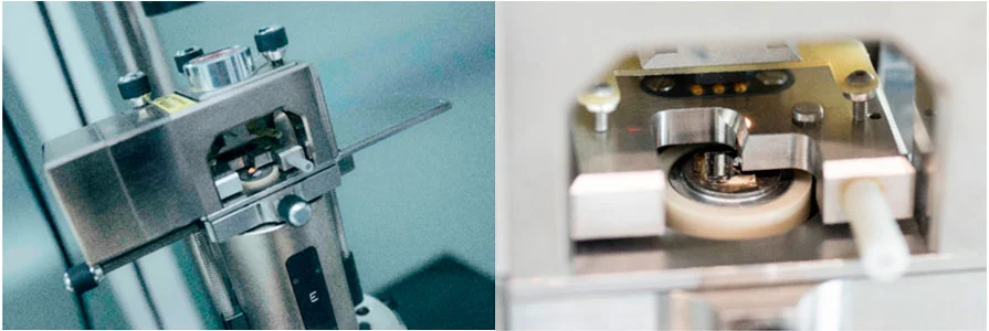
Scanning Probe Microscopy (SPM)brings together a set of techniques that do not use lenses or radiation (X-rays, electrons, etc.) to obtain high-resolution topographic images. It is an imaging tool with a wide dynamic range, spanning the realms of optical and electron microscopes. The applications are very diverse: measurements of properties such as surface conductivity, static charge distribution, localized friction, magnetic fields, and elastic modulation.
The two main forms of SPM microscopy are:
- Scanning Tunneling Microscopy (STM). Developed by Binning and Roher at IBM laboratories (Switzerland), a discovery for which they received the Nobel Prize in Physics in 1986.
- Atomic Force Microscopy (AFM) (Binning et al., 1986). This distinguishes four main modes:
Modes | Primary Aplication | Advantages | Disadvantages |
Contact | Hard surfaces, metals, ceramics, and atomic resolution on crystals. | Highest scanning speed and simplest operation. | Can damage soft samples; lateral forces wear down the tip quickly. |
Tapping (Intermittent) | Polymers, biological samples, and delicate materials in air or liquid. | Eliminates lateral (frictional) forces; Phase Imaging provides compositional contrast. | Lower scanning speed. |
Non-Contact | Extremely sensitive or reactive surfaces. | Zero tip wear; high sensitivity to long-range forces. | Very unstable in air due to surface humidity; requires vacuum for maximum resolution. |
PeakForce Tapping | Quantitative nanomechanical mapping and molecular resolution in polymers. | Ultra-precise force control; measures elasticity and adhesion at every pixel. | requires rigorous probe calibration. |
These two techniques are the ones with the highest resolving power for the study of surface structures at the atomic level. From an instrumental point of view, both techniques are very similar. STM Microscopy is applied only to conductive samples (metals or semiconductors), while AFM Microscopy can treat any type of sample (conductor, insulator, biological, etc.) and also measure their mechanical and magnetic properties at the atomic level. They are complementary techniques: STM Microscopy offers high resolution, while AFM Microscopy offers versatility.
Other variants of SPM microscopy include: Lateral Force Microscopy (LFM), Force Modulation Microscopy, Magnetic Force Microscopy (MFM), Electric Force Microscopy (EFM), Conductive AFM (C-AFM), Surface Potential Force Microscopy, Phase Imaging, Force Volume, Electrochemical STM & AFM (ECM), Scanning Thermal Microscopy (SThM), etc.
Instrumental Facilities
Scanning Probe Microscope Multimode 8, Nanoscope Feedback Unit V, Manufacturer: Veeco-Bruker
Technical Characteristics
- Approximation system: piezoelectric ceramics
- Electronic system: Feedback
- Available scanners: 140 μm, 14 μm and 1 μm (HR)
- Available techniques: AFM, STM, MFM, EFM, C-AFM, PeakForce Tapping …
- Cell for liquids
- Unit of measurement of magnetic properties
- Unit of measurement of electrical properties
- Surface conductivity measurement unit
Applications
Nanometrology and High Resolution Morphology
- Helical Polymers: Determination of chirality (direction of coiling) in single chains.
- Molecular Resolution: Measurement of interchain spacing and helix pitch in crystalline polymers.
- Measurement of surface roughness with sub-nanometric accuracy.
- Characterisation of defects, vacancies and atomic steps in crystalline networks.
Materials and Polymer Science
- Mapping of local mechanical properties (elasticity, hardness and friction).
- Study of phase separation and molecular self-assembly.
- Observation of crystallisation processes and growth of thin films.
- Analysis of adhesion forces at the nanoscopic level.
Energy and Catalysis
- Structural characterisation of photovoltaic and organic materials.
- Study of the morphology of heterogeneous catalysts and nanoparticles.
- Analysis of structural degradation in battery materials (ex-situ).
Magnetism and Conductivity
- Characterisation of magnetic domains in storage materials (MFM).
- Measurement of local electrical conductivity and tunneling currents (STM).
- Capacitance mapping in microelectronic devices.
- Charge transport analysis in conductive nanostructures.
Life Sciences and Biomedicine (For biological applications, it is highly recommended to pair the AFM with an inverted optical microscope to enable precise localization of cells or target structures and to facilitate laser alignment in liquid environments)
- Visualisation of the secondary structure of biopolymers (DNA, RNA).
- Study of the morphology of cell membranes and proteins in liquid media.
- Analysis of the rigidity and mechanics of living cells and viruses.
Observation of molecular complexes under physiological conditions.
Sample requirements
- The samples must be in good condition and therefore must not contain traces of grease, oils, or any composition that endangers the integrity of the equipment and must be non-toxic or harmful.
- Do not handle the surface of the samples with bare hands. Always wear powder-free nitrile gloves. Our recommendation, in the case of a solid sample, is that before bagging the sample in the plastic bag, it should be protected with aluminium foil (commonly used).
- Samples should be of the appropriate size (dimension) for the technique…Samples exceeding the limits should be cut.It is recommended to contact the technical staff of the Service if there are doubts about the dimensions.
- When the samples are identical on both sides, the user must indicate with a mark the side of interest. If the samples are in powder form, they can be sent in a properly sealed and identified eppendorf vial.
- Samples can be powders, fragments, sheets, solutions, dispersions,
- Upon completion of the work, the samples will be returned to the user in the way is registered on the service form. Samples not delivered to users will be kept at the Service for a stablish period. After this time, the samples will be disposed of as laboratory waste.
More information
Carmen Serra Rodríguez – Tatiana Padín Gómez – Paula Barbazán Martín
+34 986 813 882 – Fax: 986 812 135
cserra@uvigo.es – tatiana.padin@uvigo.es – pbarbazan@uvigo.es